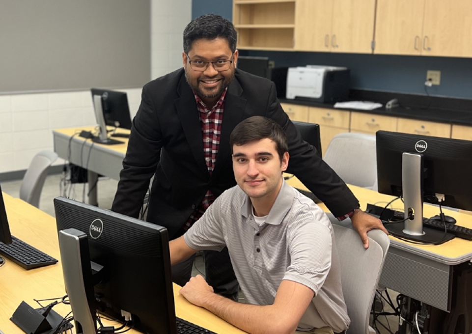
Last spring, Joseph Wikar, a senior engineering technology major at Buffalo State, was awarded a prestigious paid internship at the Center for Nanoscale Science and Technology (CNST) within the National Institute of Standards and Technology (NIST), one of the top research laboratories in the country.
He’s the second Buffalo State student to earn the competitive internship in the last three years.
“It’s great for the students and the engineering program at Buffalo State,” said Saquib Ahmed, assistant professor of engineering technology and founder and director of the Integrated Studies in Nanoscience and Nanotechnology Center, who is Wikar’s research faculty mentor. “Having students win the internship is validation for the work we’re doing in the program, and at Buff State in general.”
The internship is offered to only two or three students from more than 100 of the top schools in the country, Ahmed said. Jonathan Shaffer, ’21, one of Ahmed’s earliest research students, was awarded the internship in 2019.

Headquartered in Gaithersburg, Maryland, and operating under the U.S. Department of Commerce, the Center for Nanoscale Science and Technology houses a number of measurement and fabrication tools, as well as facilities for processing semiconductors and other nanoscale engineering processes.
Wikar landed the internship following a rigorous panel interview. The lab is headquartered in Gaithersburg, Maryland, and houses a number of measurement and fabrication tools, as well as facilities for processing semiconductors and other nanoscale engineering processes. It operates under the auspices of the U.S. Department of Commerce.
“It was a fantastic experience,” Wikar said, noting that he spent the summer in Gaithersburg. “I felt lucky that I was selected for it.”
Having two students represented in the program over the last three years was no accident, Ahmed said. He put Wikar in touch with Shaffer, so the two could discuss the internship. Ahmed is also working to create a pipeline with others who recruit for the internship.
“These guys get a large number of applications,” he said. “With the ability to get some clarity from the principal investigator, such as myself, that definitely makes the job easier.”
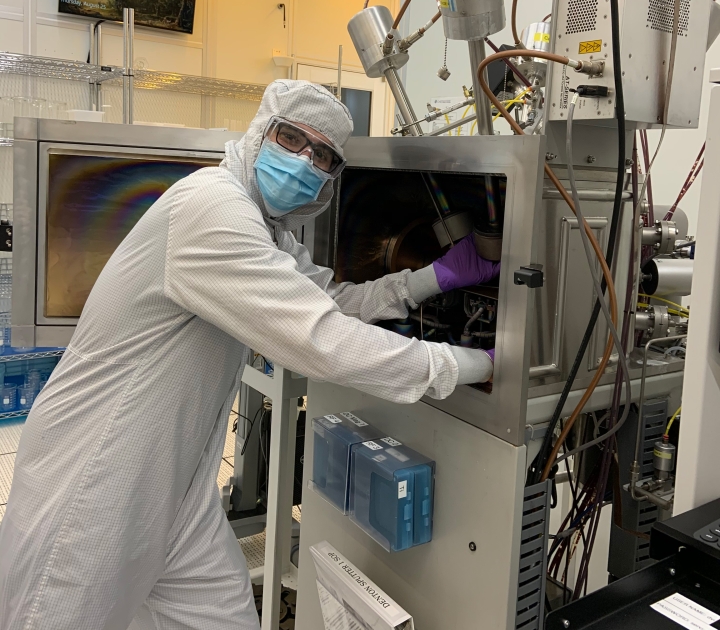
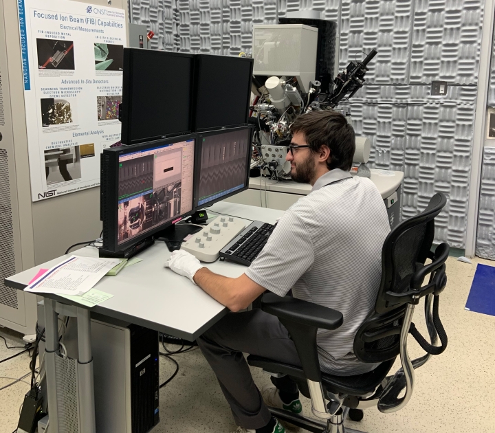
During the internship, Wikar focused on both the “maintenance” and the “processing” aspects of working on semiconductors, which are components used in electronics like computers and iPhones. He worked in the center’s clean room, where he focused on nanoscale engineering processes.
On the maintenance side, Wikar was able to work on and repair equipment that wasn’t functioning properly. He found himself working on equipment he had learned about in the classroom at Buffalo State but hadn’t had the chance to use before.
“It was cool to actually see and visualize that stuff, and get my hands on it,” he said.
“The word ‘research’ is rather vague. You’re looking at things that are not yet discovered. One of the great things about the internship is that it provides a structured atmosphere for participants.”
— Saquib Ahmed, Ph.D., Assistant Professor of Engineering Technology

On the processing side, he was involved in magnetron sputtering and e-beam evaporation, which involved taking metals and laying a thin film onto a silicon substrate.
“I also got to touch base a lot on the lithography side of things,” he said. “That was pretty interesting as well.”
One of the great things about the internship is that it provides a structured atmosphere for participants, Ahmed said.
“The word ‘research’ is rather vague,” he said. “It can end with a good outcome or it can go anywhere. You’re looking at things that are not yet discovered. With this internship, however, they’ve broken up the research work into very clear, programmable goals.”
Wikar said the equipment and processes he worked with over the summer were “cutting edge” and gave him a chance to learn about new techniques and equipment. It has also opened some doors for him for the future.
“They actually gave me the opportunity to speak with a very well-known company within the semiconductor field,” he said. “I had a really nice conversation with their CEO of American operations, and they said they’d be interested in working with me in the future,” something Wikar said he hopes to do next summer.
Overall, the internship and his studies at Buffalo State have set him up for success, he said.
“I think I’ve gained some pretty important experience where I can be an asset to any company who chooses to work with me.”
Top photo: Saquib Ahmed (left) and Joseph Wikar. Photo by Michael Canfield.
Inset photos: Joseph Wikar at the Center for Nanoscale Science and Technology. Photos courtesy of CNST.


